B13-抗反射高速 3D PCB AOI 检测设备-深圳中科精工科技有限公司
B13-抗反射高速 3D PCB AOI 检测设备-深圳中科精工科技有限公司
- 产品详情
- 产品参数
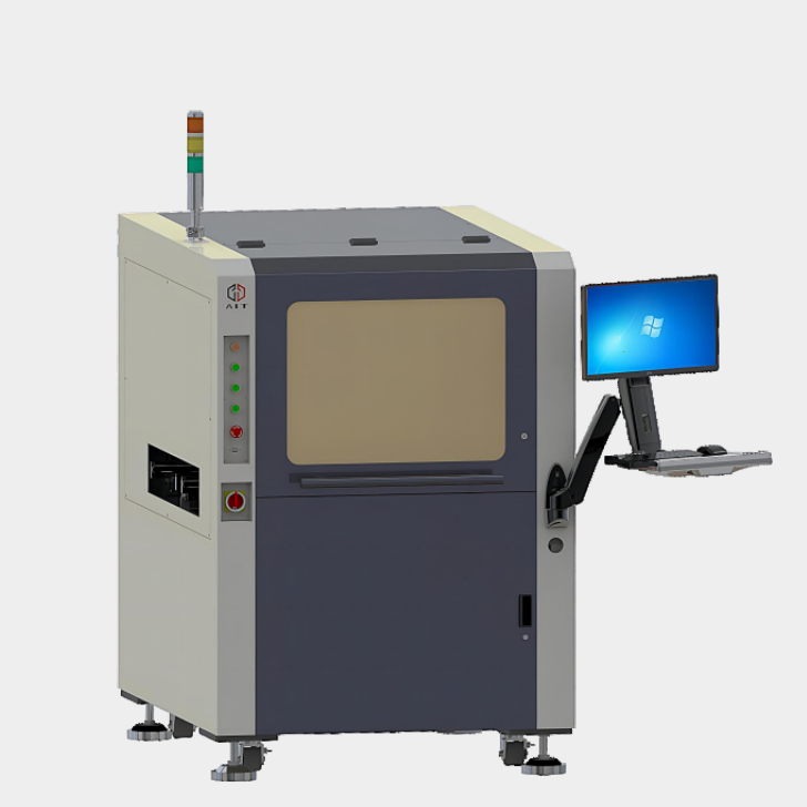
抗反射高速 3D PCB AOI 检测设备
Anti-reflex high-speed 3D PCB AOI detection device
深圳中科精工科技有限公司
Shenzhen Zhongke Jinggong Technology Co.,LTD
一、产品介绍
抗反射高速3D PCB AOI检测设备 是通过人工上下料,直线模组移栽PCB来回运动,3D相机拍照取像来自动检测PCB板的3D缺陷。
产品主要采用结构光3D视觉系统+4个侧面相机,通过3D形状匹配、AI、残差分析、2D AI分析、色域分析、OCV、OCR等检测算法,提取PCB板元件布局、颜色、亮度2D信息及3D形貌等,自动检测PCB板的缺陷。检测内容为破损、反向、缺件、偏移、立碑、歪斜、翻件、侧立、高度误差、翘起、多锡少锡、虚焊、外观不良、其他3D尺寸误差、字符识别等60多种缺陷。
抗反射高速3D PCB AOI检测设备目标是解决3D PCB检测技术中出现强反射、区域阴影,且检测速度慢、准确度低等问题。产品在技术方案上采取了独树一帜的抗反射高速3D 重构算法,在检测速度、准确度核心指标上优势明显。已经实现了初步和头部企业的批量验证,目前国内市场占有率达到18%,预计经过3年市场拓展可以实现市场占有率40%以上。
抗反射高速3D PCB AOI检测设备解决了我国高端PCB制造业的痛点问题,结束对国外设备的依赖局面,可替代国际头部企业韩国高迎、MIRTEC、Parmi,日本Saki、Yamaha、Omron的设备,突破了强反射和区域阴影关键难题,且检测速度、准确度均优于国际对标企业。
二、性能参数:
1.设备尺寸:1020*1400*1750mm
2.设备重量:≈950kg
3.运动系统:
a.XY移动平台:X行程:550mm;Y行程:800mm;X/Y精度:±2um
b.Z向精密顶升平台:Z向精密顶升平台顶升PCB载具上升和下降、顶升精度可达到+/-0.02mm
4.产品净高:PCB板最大弯曲≤5mm,正面间隙45mm、反面间隙50mm
5.产品兼容:最大尺寸500*450mm,厚度0.2-0.5mm,重量≤3KG,支持顶针配件
6.检测精度:
a.高度方向:最小器件厚度:15mm;分辨率:0.1um;重复测量精度:3um
b.水平方向:最小尺寸:7.1um/Piexl
7.编程方式:根据标准产品误差分析、Gerber或CAD导入
8.光学系统:2500万大靶面相机+高景深远心镜头;4个白光投影仪;4个侧面1200万监控相机;8段彩色LED光源。
9.性能:
a.能检测的PCB最大尺寸范围大于 500mm×450mm;
b.具有3D检测技术,高程精度±3μm;
c.2500万像素相机,3D 最快检测速度 720mm2 /sec;
d.2500万像素相机,2D 最快检测速度 2800mm2 /sec;
e.PCB 板正面间隙 45mm;
f.PCB 板反面间隙 50mm;
g.物距可调,视觉系统高度手动可调;
h.最大PCB板厚度0.5mm~5mm;
i.最高器件厚度15mm;
j.最小测量尺寸7μm;
k.常规缺陷漏检率0%,虚焊漏检率不高于0.1%;
l.常规过检率 3%,虚焊过检率不高于5%。
10.功能:
a.3D立体成像功能;
b.实时成像功能;
c.产品形貌比对;
d.电装缺陷检测功能;
e.3D AOI 缺陷检测、分类功能;
f.三防加固后缺陷检测功能;
g.全自动检测功能;
h.缺陷提示方式可设置,可自动报警并停止检查,或者记录后继续检查;
i.图像数据记录功能,可按产品类型和编号分文件夹存放;
j.在辅助下,产品编号自动识别和提取;
k.二维码扫描记录功能;
l.根据甲方提供的板卡参数(不少于8款)协助建立3D辅助检测模型,提升检测速度,提高检测准确度;
m.用户灵活配置功能。
11.电气
a.电源:单相 200~240V,50~60Hz,不大于 1.5KW;
b.空气压力:0.5Mpa。
12、软件
a.内置 SPC、内置修复软件,服务器系统;
b.自动制定PCB板及拼板扫描方案,自动根据类别属性生成板上元件的检测方案、检测项目、检测窗口、检测算法,并允许人工调整;
c.可本地和远程定制检测方案;
d.无人值守全自动执行检测;
e.图表化显示缺陷统计分析结果,数据库永久可追溯;
f.具备维修站功能,允许人工复检。
13.针对缺陷类型
a.常规缺陷
漏焊、掉件、缺件、偏移、歪斜、立碑、侧立、翻件、错件、破损、
连锡、虚焊、IC脚虚焊、OCR、高度、位置&角度、爬锡、多锡、少锡、尺寸、异物、翘起、图像拼接、条形码、二维码 共25种缺陷。
b.其他非常规缺陷
桥接、极性、焊料堆积、松香焊、过热、冷焊、松动、拉尖、针孔、气泡、铜箔翘起、剥离、空洞、不对称、浸润不良、IC翘脚、漏漆、双芯片、BGA翘起、锡珠 共20种缺陷。
1. Product presentation
The anti-reflection high-speed 3D PCB AOI detection equipment automatically detects the 3D defects of the PCB board by manual loading and unloading, taking pictures of the 3D camera by transplanting the PCB and moving the 3 D module with the PCB.
The product mainly adopts structured light 3D vision system + 4 side cameras, through 3D shape matching, AI, residual analysis, 2D AI analysis, color gamut analysis, OCV, OCR and other detection algorithms, extract the PCB element layout, color, brightness 2D information and 3D morphology, automatically detect the defects of PCB board. The detection contents include more than 60 defects, such as damage, reverse, missing parts, offset, monument, skew, flip, side stand, height error, warping, more than tin and less tin, deficiency welding, poor appearance, other 3D size error, and character recognition.
The goal of anti-reflection high-speed 3D PCB AOI detection equipment is to solve the problems of strong reflection, regional shadow, slow detection speed and low accuracy in 3D PCB detection technology. The product adopts a unique anti-reflection high-speed 3D reconstruction algorithm, which has obvious advantages in the core indicators of detection speed and accuracy. It has realized the batch verification of preliminary and head enterprises, the current domestic market share has reached 18%, and it is expected that the market share can be more than 40% after 3 years of market expansion.
Anti-reflection high-speed 3D PCB AOI detection equipment solves the pain points of high-end PCB manufacturing, end of the dependence on foreign equipment, can replace international head enterprise Korea high meet, MIRTEC, Parmi, Japan Saki, Yamaha, Omron equipment, broke through the strong reflection and regional shadow key problem, and detection speed, accuracy are better than the international companies.
2. Performance parameter:
1. Equipment size: 1020*1400*1750mm
2. Equipment weight: 950kg
3. Movement system:
a. XY mobile platform: X travel: 550mm; Y travel: 800mm; X/Y accuracy: ± 2um
b. Z to precision jacking platform: Z to precision jacking platform jacking PCB vehicle increases and decreases, and the jacking accuracy can reach + / -0.02mm
4. Product net height: PCB board maximum bending 5mm, front clearance 45mm and reverse clearance 50mm
5. Product compatibility: maximum size 500 * 450mm, thickness 0.2-0.5mm, weight 3 KG, support thimble accessories
6. Detection accuracy:
a. Height direction: minimum device thickness: 15mm; resolution: 0.1um; repeated measurement accuracy: 3um
b. Horizontal direction: minimum size: 7.1um / Piexl
7. Programming method: according to the standard product error analysis, Gerber or CAD import
8. Optical system: 25 million large target face camera + high view deep heart lens; 4 white light projectors; 4 side 12 million surveillance cameras; 8 segment color LED light source.
9. Performance:
a.The maximum size range of PCB that can be detected is greater than 500mm 450mm;
b.With 3D detection technology, the elevation accuracy of ± 3 μm;
c.25 megapixel camera, 3D fastest detection speed of 720mm2 / sec;
d.25 megapixel camera, 2D fastest detection speed 2800mm2 / sec;
e.PCB board front clearance of 45mm;
f.Negative clearance of PCB board is 50mm;
g.The material distance is adjustable, and the visual system height is manually adjustable;
h.Maximum PCB, plate thickness of 0.5mm~5mm;
i.Maximum device thickness is 15mm;
j.Minimum measurement size: 7 μm;
k.The missed detection rate of conventional defects is 0%, and the missed detection rate of deficiency welding is not higher than 0.1%;
l.The conventional inspection rate is 3%, and the false welding inspection rate is not higher than 5%.
10. Functions:
a.3D stereoscopic imaging function;
b.Real-time imaging function;
c.Product morphology comparison;
d.Denso-mounted defect detection function;
e.3D AOI Defect detection and classification function;
f.Defect detection function after three prevention and reinforcement;
g.Automatic detection function;
h.The defect prompt mode can be set, which can automatically alarm and stop checking, or continue to check after recording;
i.Image data recording function can be stored according to product type and number;
j.Under the assistance, the product number is automatic identification and extraction;
k.QR code scanning and recording function;
l.Assist in the establishment of 3D auxiliary detection model according to the board card parameters provided by Party A (no less than 8 items) provided by Party A to improve the detection speed and improve the detection accuracy;
m.Users can flexibly configure the functions.
11. Electrical
a.Power supply: 200~240V, 50~60Hz, not more than 1.5KW;
b.Air pressure: 0.5 Mpa.
12. Software
a.Built-in SPC, built-in repair software, server system;
b.Automatically formulate the PCB board and panel scanning scheme, automatically generate the detection scheme, detection items, detection window and detection algorithm of the components on the board according to the category attributes, and allow manual adjustment;
c.The detection scheme can be customized both locally and remotely;
d.Unattended and fully automatic detection;
e.Chart shows the defect statistical analysis results, and the database is permanently traceable;
f.With the function of a maintenance station, allowing manual reinspection.
13. For the defect type
a.Conventional defects
Leak welding, missing, missing, missing, offset, skew, monument, side, turning, wrong, wrong, damaged,
Tin, deficiency welding, IC foot deficiency welding, OCR, height, position & Angle, climbing tin, more tin, less tin, size, foreign body, warping up, image stitching, barcode, QR code a total of 25 defects.
b.Other unconventional defects
There are 20 defects of bridging, polarity, accumulation of solder, rosin welding, overheating, cold welding, loosening, pulling point, pinhole, bubble, copper foil warping, peeling, cavity, asymmetry, poor infiltration, IC, foot warping, paint leakage, double chip, BGA warping, and tin bead.
请为我们投下宝贵的一票,谢谢!
Please vote for us, thank you!